


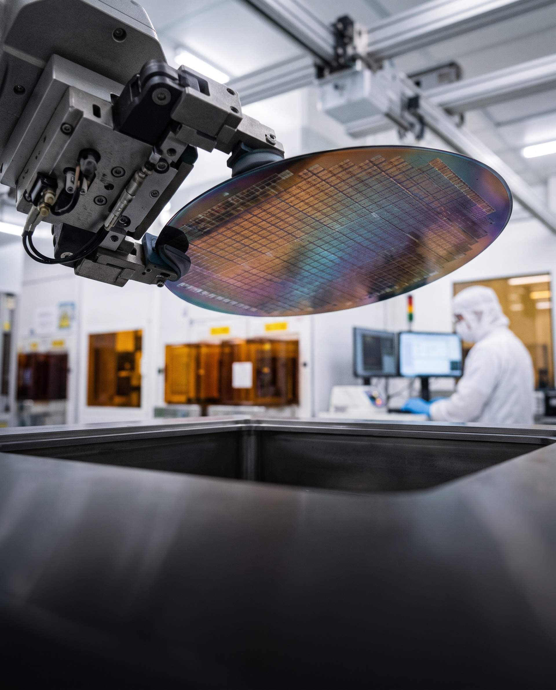
Taiwan Semiconductor Manufacturing Company has achieved a major milestone in advanced chip manufacturing, delivering its first commercial validation silicon samples built on its 1.6-nanometer fabrication process, officially designated as the A16 technology node.
The delivery of early test wafers to key architectural partners marks a critical step forward in semiconductor physics. As global tech giants construct massive clusters of computing servers to train multimodal artificial intelligence models, traditional chip architectures have run into severe physical roadblocks involving electrical resistance and heat dissipation. TSMC's A16 node directly tackles these bottlenecks by introducing groundbreaking engineering solutions that bypass decades-old chip layout constraints.
The Breakthrough of Backside Power Delivery
The defining innovation of the A16 process is the commercial implementation of Super Power Rail technology, widely known across the microelectronics industry as backside power delivery.
In conventional microchips, electrical power lines and complex signal transmission wires are crammed together on the front side of the silicon wafer directly above the microscopic transistors. As transistors shrank down to atomic dimensions, this crowded arrangement created severe electrical interference, voltage drops, and wasted energy, limiting how fast processors could run.
With backside power delivery, TSMC engineers flipped the script. They relocated the entire power distribution network to the underside of the silicon wafer, connecting power lines directly to the transistors from behind. This radical structural separation leaves the front side entirely clear for signal routing, eliminating signal noise, reducing wire resistance, and allowing transistors to be packed roughly ten percent tighter together.
Massive Speed and Energy Gains for AI Clusters
According to technical performance metrics released by TSMC, the A16 process delivers an eight to ten percent increase in clock speed at the same power consumption compared to its earlier two-nanometer nodes. Alternatively, chip architects can choose to run processors at identical speeds while slashing overall energy use by fifteen to twenty percent.
For hyperscale data center operators like Microsoft, Google, Meta, and Nvidia, these efficiency gains translate into enormous financial and operational advantages. Modern AI data centers consume gigawatts of electricity, with cooling and power delivery representing their biggest single operating cost. Squeezing higher computing throughput out of smaller, more power-efficient silicon dies allows cloud operators to run advanced neural network inference at lower temperatures and reduced operational expense.
Advanced Packaging and Memory Integration
The physical leap in silicon fabrication is closely paired with next-generation modular packaging technologies. TSMC confirmed that the A16 process is fully optimized for its Chip-on-Wafer-on-Substrate packaging platforms, allowing multiple compute chiplets to connect directly with High-Bandwidth Memory stacks.
By bringing processors and high-speed memory within fractions of a millimeter of each other on an ultra-dense silicon interposer, data transfer bottlenecks between computing cores and memory are virtually eliminated. This tight integration is essential for training frontier foundation models with hundreds of billions of parameters, where memory bandwidth often limits real-world computing speeds more than raw processor cycle rates.
Scaling Microelectronics Into the Angstrom Era
Developing sub-two-nanometer silicon requires extraordinary lithographic precision. TSMC utilizes advanced extreme ultraviolet lithography systems capable of etching features measured in angstroms, or fractions of a nanometer. At this scale, atomic-level quantum mechanical effects come into play, requiring new gate-all-around nanosheet transistor architectures to prevent electrons from leaking across microscopic barriers.
The successful production of early A16 validation silicon demonstrates that Moore's Law continues to progress through ingenious material engineering, even as traditional silicon scaling nears fundamental physical limits.
Commercial Timelines and the Race Ahead
TSMC confirmed that initial risk production for the A16 process will ramp up over the next eighteen months, with full-scale commercial volume manufacturing scheduled to begin in the second half of 2026. The milestone puts heavy pressure on rival chip foundries, including Intel and Samsung Electronics, which are rushing to deploy their own competing backside power nodes.
As the international race to build sovereign AI infrastructure intensifies, the arrival of 1.6-nanometer silicon ensures that hardware builders will possess the computational density needed to power the next leap in autonomous intelligence.




Comments
0